Fig. 1.
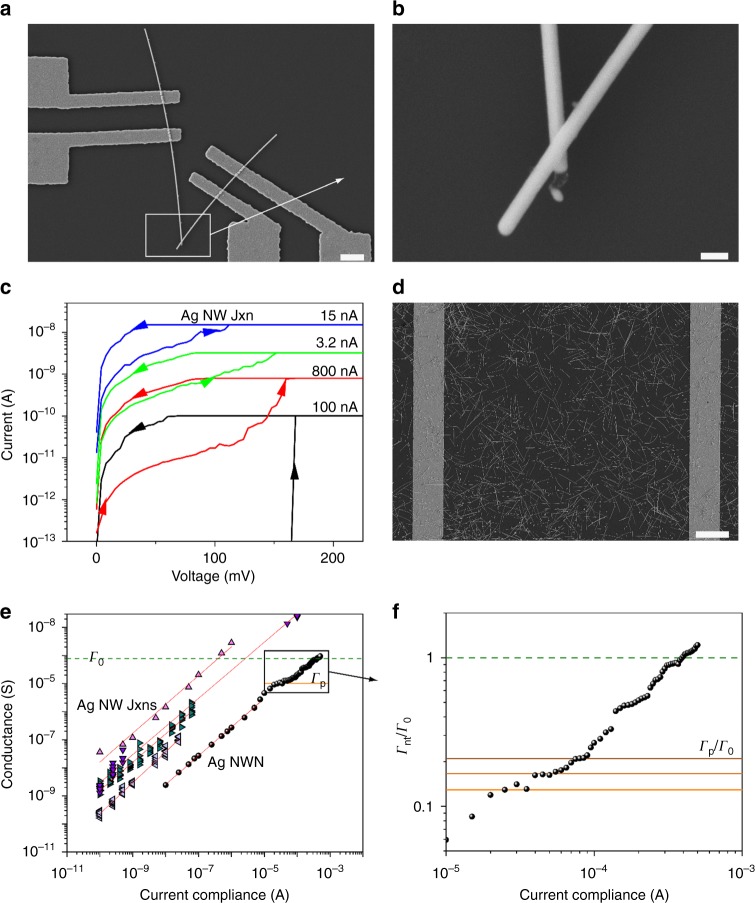
Electrical characterization of nanowire systems. a Scanning electron microscopy (SEM) image of an Ag nanowire junction (NW Jxn) contacted with four electrodes by electron beam lithography. The white scale bar represents 1 µm. b A magnified SEM image of the two overlapping Ag NWs. The scale bar corresponds to 100 nm. c I–V curves for different programmed compliance currents for a single Ag NW Jxn. d SEM image of an Ag nanowire network (NWN). The white scale bar corresponds to 10 µm. All networks studied here have nearly the same wire density of approximately 0.4 wires/μm2. e Conductance plotted against the current compliance (log–log scale) for numerous Ag NW systems. Ag NW Jxns are represented by diamond symbols whereas circles show the measurements for a 500 × 500 µm Ag NWN. The solid lines correspond to power law fits of these datasets. Both systems (Jxn and NWN) display a power-law dependence, however the Ag NWN shows a break from this trend below Γ0 (the quantum of conductance) shown as the horizontal dashed green line. Measurement methods are detailed in Supplementary Figures 1 and 2. f Zoom-in at the high current compliance range of the Ag NWN conductance (Γnt) taken from panel e and divided by Γ0. This dataset was obtained using an extremely fine current compliance sampling in order to detect the numerous conductance plateaus marked by the solid horizontal lines. The green dashed line depicts the quantum of conductance. The orange horizontal line indicated the first conductance plateau (Γp) found at , which gives . Subsequent plateaus appear at and

