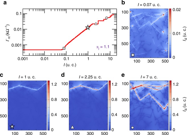
Fig. 3.
Simulated conductance evolution of an Ag nanowire network (NWN). a The same conductance versus current curve shown in Fig. 2 for the Ag NWN template depicted in the Supplementary Figure 7. The junction characteristics are set at and . The symbols mark points in the curves in which current colour maps were taken. b–e Current colour maps calculated over each wire segment (Is) of the Ag NWN. Snapshots were taken for four sourced current values specified on the top of each current map and distinguished by the symbols: square (transient growth), star (power-law), triangle and circle (both set in the post-power-law regime). In particular, the post-power-law state at u.c. is located at the first conductance plateau, . Animations revealing the complete evolution of the network in response to the current source, junction optimization of the top-three paths of least-resistance, and current-segment maps are provided in the supplemental material (cf. Supplementary Note 3 and Supplementary Figure 9 for animation description)

