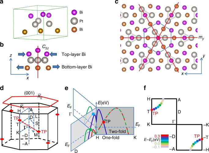
Fig. 1.
Crystal structure and schematic electronic structure. a Three-dimensional crystal structure of trigonal layered PtBi2. Top and bottom layers of Bi are labeled with different colors. b Side view of the lattice showing C3z rotation symmetry. Shrinking of top Bi layer and extension of bottom Bi layer result in a lack of an inverse center of trigonal layered PtBi2. c Top view of lattice showing my mirror symmetry; other two mirror reflection symmetries are obtained by rotating the top Bi atom. d Three-dimensional bulk Brillouin zone (BZ) and (001) surface BZ with high-symmetry points are indicated. Red spots indicate TPs. Red-dashed line connects a pair of TPs. e Schematic band structures along three different high-symmetry lines. Red spots at the crossing points along line H–K indicate the TPs. The light blue and green spots along H–Г and H–D are doubly degenerate points. Curves of mixed red and green color represent doubly degenerate bands (twofold) and those of single color represent nondegenerate bands (onefold). f Tracks of degenerate point around the Fermi level in H–K–Γ–A plane. Colors of the spots represent the energy relative to the Fermi energy EF. The point at line H–K is a TP, and the points off the H–K line are doubly degenerate

