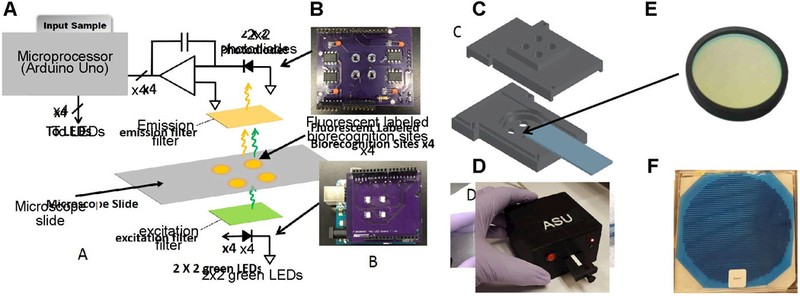
Figure 2:

Schematic, prototype board, CAD design, and filters in a 2×2 array fluorescence detection platform. (A) Circuit schematic showing charge-integration amplifier readout circuit, 2×2 biorecognition sites on a microscope slide and LEDs used as the excitation source (B) Printed circuit board (PCB) showing 2×2 photodiode and amplifiers as well as the 2×2 LEDs soldered (C) 3D printed optical assembly showing apertures for excitation sources, holders for filters, slot for microscope slide, and aperture to fit photodiodes on the top piece (emission filter slot on reverse side) (D) Stacked microcontroller board, PCBs, and 3D printed assembly packaged in a 3D printed enclosure (E) 25 mm filter typically used in fluorescence microscopy; arrow points to 25.3 mm diameter slot in 3D printed assembly shown (F) 6 inch filter dielectric stack deposited on a 1 mm thick substrate and diced to ∼3×3 mm (not to scale).
