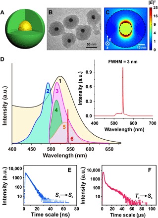
Fig. 1. Demonstration of a three-level spaser.

Schematic structure (A), TEM (B), and FDTD-simulated electric field distribution (C) images of the Au@dye/SiO2 nanoprobe [yellow core and green layer in (A) denote the Au core and the outer dye-doped SiO2 layer, respectively]. (D) Plasmon resonance absorption (1), excitation (2), spontaneous emission (3), split spontaneous emission S1→S0 (4) and T2→S0 (5), and stimulated emission (6) curves of the nanoprobe. Inset in (D) is the observed stimulated emission spectrum of the nanoprobe. Emission lifetime of S1→S0 (E) and T2→S0 (F) by using the dye. a.u., arbitrary units; FWHM, full width at half maximum.
