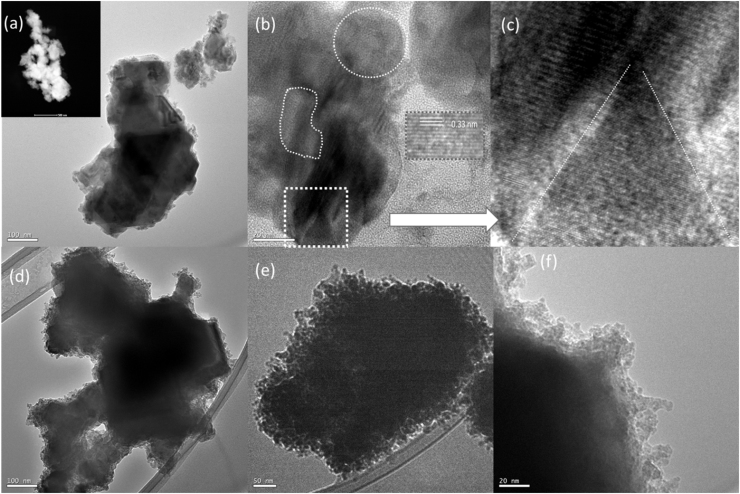
Fig. 5.
TEM images of Cu2±xSe nano/microcrystals produced at (a-c) 200, and (d-f) 260 °C reaction temperatures. (a) Low magnification TEM image scale bar 100 nm. (Inset) high angle annular dark field (HAADF) scanning transmission electron microscopy (STEM) image of NCs (b) high magnification; scale bar 20 nm; (Inset) HRTEM shows lattice fringes with an inter-planner spacing of ∼ 0.33 nm, and (c) enlarged view of the squared portion of the image (b). TEM images of copper selenide NCs produced at 260 °C at (d) low; scale bar 100 nm, and (e, f) at higher magnifications; scale bar 50 and 20 nm.

