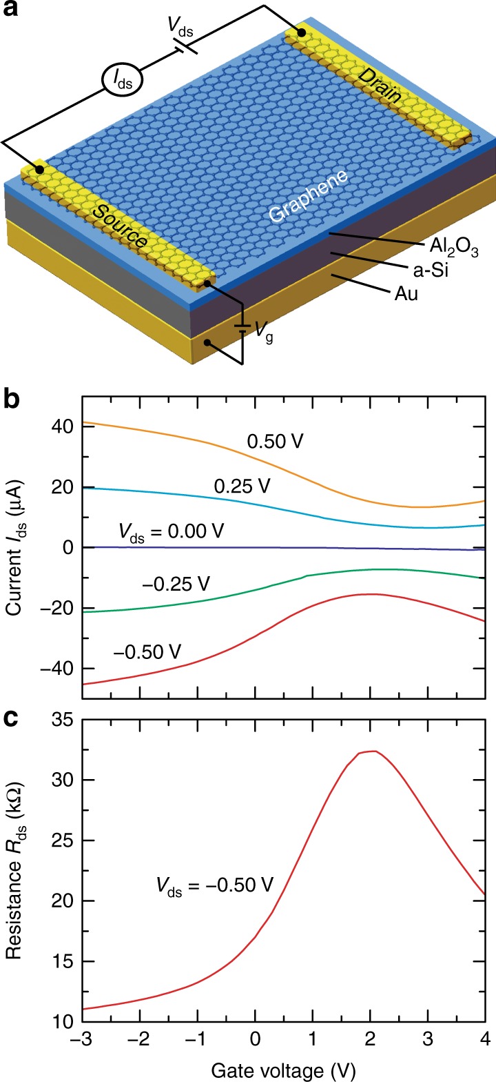
Fig. 1. Tuning graphene conductivity with a low gate voltage bias.

a Schematic of the FET structure in which a-Si serves as part of the back-gate electrode and the ultrathin Al2O3 layer serves as the gate dielectric. b Measured drain-source current Ids across the graphene as a function of gate voltage Vg at different drain-source biases Vds. c Graphene resistance Rds as a function of gate voltage at Vds = −0.50V, revealing the graphene charge neutrality point at approximately 2 V
