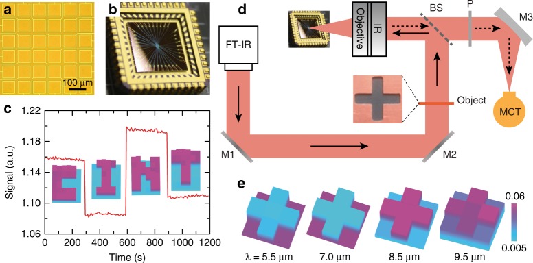
Fig. 5. Hybrid graphene metasurface spatial light modulator.
a An optical micrograph showing the active area consisting of an array of 6 × 6 functional pixels. b A photograph of the device after being wire-bonded to a chip carrier. c Spatial reflection patterns of “CINT” at λ = 8.3 μm by selectively applying gate voltages Vg = −3 V (‘OFF’) and +7 V (‘ON’) to individual pixels in accordance with the patterns shown by the images in the insets (purple color indicates ‘ON’). Changes among SLM patterns result in different measured signal intensities from the single-pixel detector. The images in the insets are taken by raster-scanning pixels, i.e., the corresponding pixel is either ‘ON’ or ‘OFF’ while all other pixels remain ‘OFF’. d Schematic of the single-pixel imaging setup employing the hybrid graphene metasurface spatial light modulator. M1 and M2 flat mirrors, BS beam splitter, P polarizer, M3 parabolic mirror, and MCT mercury-cadmium-telluride single-pixel detector. e Reconstructed images of a cross-shaped object using a raster-scan measurement matrix at different wavelengths of λ = 5.5 μm, 7 μm, 8.5 μm, and 9.5 μm

