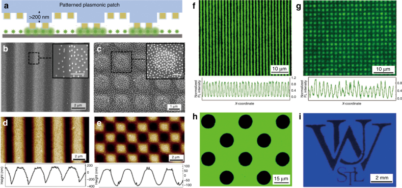
Fig. 3. Patterned plasmonic patch and localized fluorescence enhancement.
a Schematic showing a patterned plasmonic patch, which selectively enhances the fluorescence in the regions of conformal contact. In all of the used patterns, the height of the surface-relief portions is >200 nm. SEM image of a (b) stripe array and (c) square lattice PDMS with Au@Ag-490 adsorbed (insets show zoomed-in SEM images of the highlighted area revealing a uniform distribution of the plasmonic nanostructures on both elevated and surface-relief regions; inset scale bars represent 500 µm). AFM images of (d) stripe array (z scale: 430 nm) and (e) square lattice (z scale: 200 nm) plasmonic patches revealing the height profile of the surfaces. Fluorescence images of an FITC-coated silicon surface with (f) stripe array and (g) square lattice plasmonic patches on top. The plots below reveal the fluorescence intensity profiles. h Fluorescence map of FITC with a plasmonic patch (with Au@Ag-490 adsorbed) with circular pores. i Fluorescence image (CW800) of the “Washington University in St. Louis” logo obtained using a plasmonic patch (with AuNR-760 adsorbed) with an engraved logo

