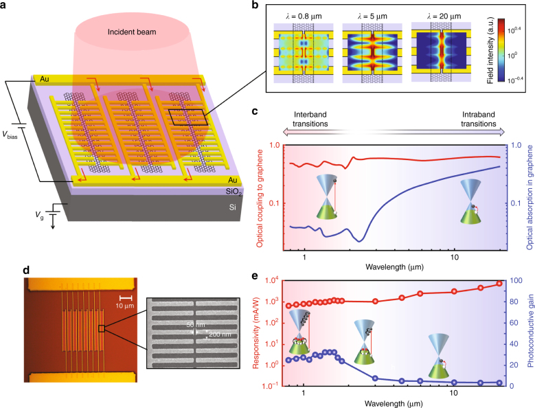
Fig. 1.
High-responsivity and broadband photodetection via gold-patched graphene nano-stripes. a Schematic of a photodetector based on gold-patched graphene nano-stripes. The photodetector is fabricated on a high-resistivity Si substrate coated with a 130-nm-thick SiO2 layer. The gate voltage applied to the Si substrate, Vg, controls the Fermi energy level of the graphene nano-stripes. The gold patches have a width of 100 nm, periodicity of 200 nm, height of 50 nm, length of 1 μm, and a tip-to-tip gap size of 50 nm. b Color plot of the transmitted optical field, polarized normal to the graphene nano-stripes, through the gold patches at 0.8, 5, and 20 μm, indicating highly efficient and broadband optical coupling to the graphene nano-stripes. c Numerical estimates for the optical coupling (red curve) and optical absorption (blue curve) in the graphene nano-stripes as a function of wavelength. d Optical microscope and scanning electron microscopy (SEM) images for a fabricated photodetector based on gold-patched graphene nano-stripes. e The measured responsivity (red data) and photoconductive gain (blue data) of the fabricated photodetector at an optical power of 2.5 μW, gate voltage of 22 V, and bias voltage of 20 mV

