
Fig. 2. Design of silicon photonic crystal using a bowtie-shaped unit cell.
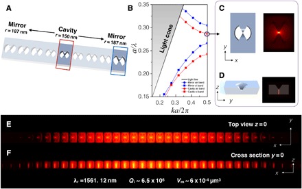
(A) The cavity is formed with a center unit cell of 150 nm radius and mirror unit cells of 187 nm radii on both sides of the cavity. The radius is gradually tapered from the center to the mirror segments. The photonic crystal lattice spacing is a = 450 nm, and the width of the waveguide is 700 nm. The structure is designed with a 220-nm silicon device layer and a 2-μm-thick buried oxide layer. (B) Optical band structures of the cavity unit cell (red curve) and mirror unit cell (blue curve). (C) Top view (xy plane) and (D) cross-sectional view (yz plane) schematics and associated air band edge electrical energy in the center unit cell. (E) Log plot of the photonic crystal cavity electric energy distribution at the resonance wavelength in the xy plane at z = 0 (v-groove tip). (F) Log plot of the photonic crystal cavity electric energy distribution at the resonance wavelength in the xz plane at y = 0 (bowtie tip). Figure S2 (A and B) shows the same mode profiles using a linear scale.