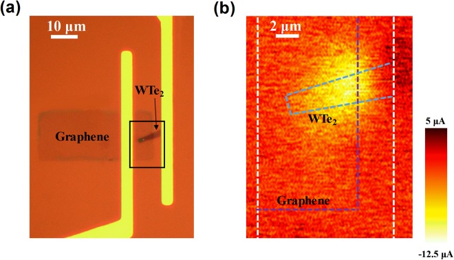
Figure 3.
A staggered graphene/WTe2 heterostructure device and photocurrent mapping. (a) An optical micrograph of the device, with graphene is staggered on top of WTe2 flake. The area inside the black square is the scanned area. (b) Scanning photocurrent micrograph of the device acquired at VDS = 0.1 V, with 0.6 μW power at 532 nm. Regions of photocurrent are observed in the overlapping area outlined by the WTe2 flake (blue) with the patterned graphene film (purple). The electrodes are indicated by white dashed lines.

