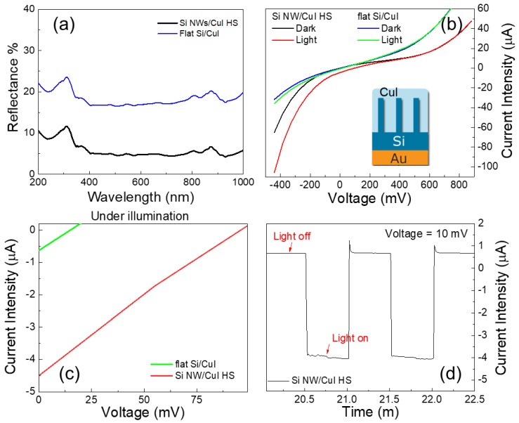
Figure 5.
(a) Reflectance measurements of flat Si /CuI and Si NWs/CuI junctions are reported in blue and black, respectively (b) I-V characteristic of both Si/CuI and Si NWs/CuI n-p heterojunction investigated under dark and light illumination conditions. The inset shows the schematic of the Si NWs/CuI device contacting during the I-V characterization. (c) PV output characteristic of the n-p Si/CuI and Si NWs/CuI devices tested under light illumination are show in green and red, respectively. (d) Current intensity measured in the device biased at 10 mV under dark/light pulses modulated by intervals of 25 s.

