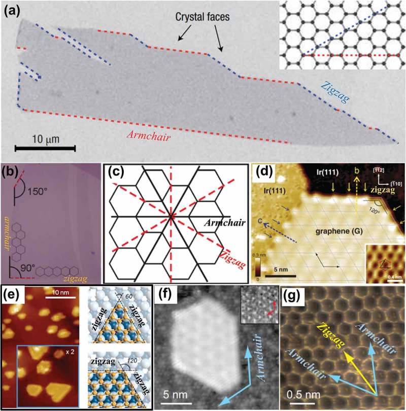
Figure 5.

(a) Scanning electron microscopy (SEM) image of a relatively large graphene crystal, which shows that most of the crystal’s faces are zigzag and armchair edges, as indicated by blue and red lines and illustrated in the inset [7]. (b) A typical graphene flake obtained by micromechanical cleavage [72]. (c) Sketch of the honeycomb crystal lattice of graphene. Two distinct crystallographic orientations of a graphene crystal, rotated against each other in multiples of 30°, are indicated as armchair type (solid lines) and zigzag type (dashed lines) [72]. (d) CC-STM image of edges of graphene on Ir(111), with crystallographic directions of the Ir substrate denoted at the top-right side [89]. (e) STM image of graphene structures on Co substrate, and schematic of triangular and hexagonal corners, respectively, for zigzag-edged graphene structures on Co(0001) [90]. (f) 20 × 20 nm2 STM image and (g) 2.5 × 2.5 nm2 rendered STM topography of graphene island on 6H-SiC(0001) substrate. Overlaid on this image are the two lowest energy edge directions: zigzag (yellow arrow) and armchair (blue arrows) [75] (reused with permissions from [7] Copyright © 2007, Springer Nature, [72] Rights managed by AIP Publishing, [89] Copyright © 2012 American Physical Society, [90] Copyright © 2014, American Chemical Society, and [75] Copyright ©2010 American Physical Society.).
