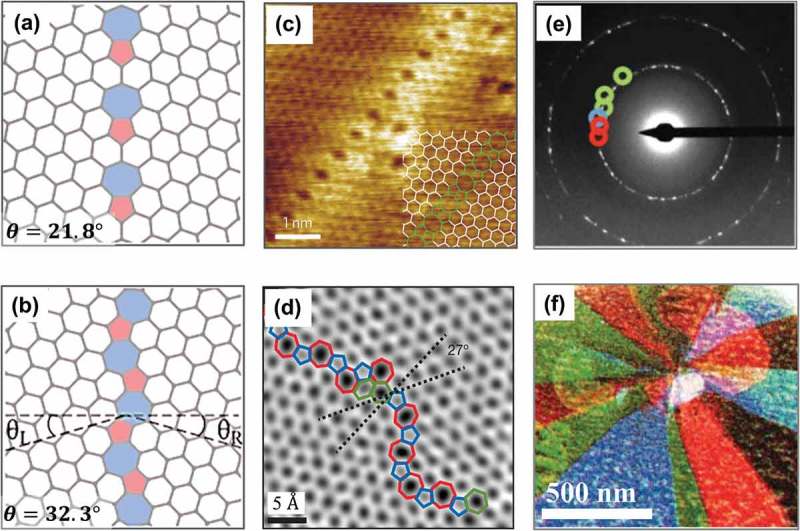
Figure 13.

Configurations of (a) the θ = 21.8° and (b) the θ = 32.2° symmetric large-angle GBs, respectively [137]. (c) STM image of a regular line defect in graphene on the Ni(111) [208]. (d) Aberration-corrected annular ADF-STEM image of two grains which intersect with a relative rotation of 27°, and are stitched together by an aperiodic line of dislocations [209]. (e) Electron diffraction pattern obtained by DF-TEM imaging graphene grains one by one with few-nanometer resolution using an objective aperture filter in the back focal plane through a small range of angles, and repeating this process using several different aperture filters. (f) False-color, DF image overlay of the sizes, shapes and orientations of several grains [209] (reused with permissions from [137] Copyright © 2014, Springer Nature, [208] Copyright © 2010, Springer Nature, and [209] Copyright © 2011, Springer Nature.).
