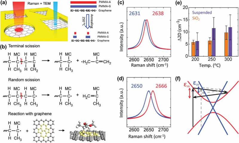
Figure 18.

(a) Schematic illustration of a combination of TEM observation and Raman spectroscopy for graphene. PMMA-A and PMMA-G correspond to PMMA facing the air and graphene respectively. Comparisons of the 2D peak positions before and after annealing for (c) Si-supported and (d) free-standing CVD graphenes. (e) Histogram of the Δ2D as a function of annealing temperature for both Si-supported and free-standing graphenes. (f) Schematic illustration of the electronic structure near the Dirac points of pristine (linear) and annealed (parabolic) CVD graphenes. All pictures are extracted from Ref [329] (reused with permission from [329] Copyright © 2012, American Chemical Society.).
