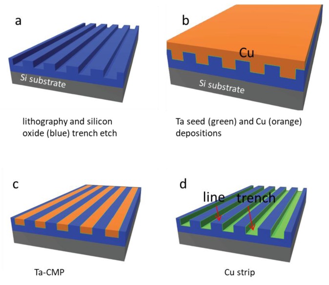
Figure 1.
Schematic illustration of processing flow for tantalum (Ta) polished specimens. Parallel line/trench patterns were transferred to the silicon oxide thin film (blue) by lithography and dry etch techniques shown in (a). This is followed with Ta and copper (Cu) film depositions on the patterned structures in (b). Excess copper was then removed by using the copper and then followed with barrier metal chemical-mechanical polishing (CMP) in (c). The final step in (d) is copper strip by nitric acid.

