Fig. 3.
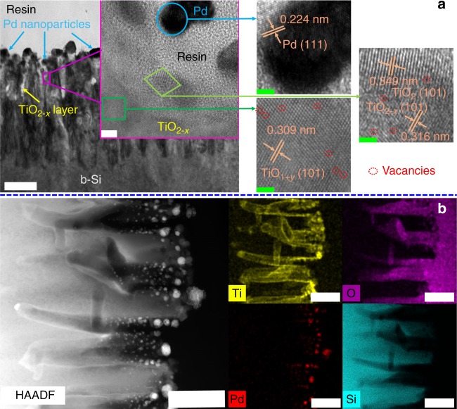
Microstructure and composition distribution of Pd/b2-TiO2/b-Si. a Cross-sectional TEM image and related high-magnification images of Pd/b2-TiO2/b-Si. The scale bar label is 200 nm in TEM image. The inset in TEM image is the magnification image of the specified area by HRTEM with the scale bar label of 5 nm. High-magnification images on the right correspond to the marked area in the inset with the scale bar label of 2 nm. b HADDF-STEM image with matching elemental distribution map for Pd/b2-TiO2/b-Si. Ti, O, Pd, and Si are represented as yellow, purple, red, and Cambridge blue, respectively. All the scale bar labels are 200 nm

