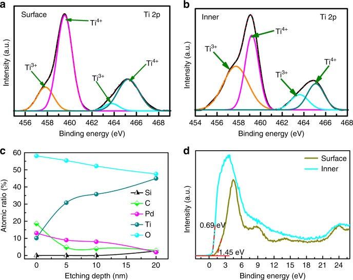
Fig. 4.
XPS depth profiling of Pd/b2-TiO2/b-Si. a Ti 2p spectrum for the surface of Pd/b2-TiO2/b-Si. b Ti 2p spectrum for the inner of Pd/b2-TiO2/b-Si after the etching depth of 20 nm. c Elemental depth profile of Pd/b2-TiO2/b-Si. d XPS VB spectra of the surface and inner (etching depth of 20 nm) of Pd/b2-TiO2/b-Si. It must be mentioned that the extra C 1 s peak at 284.8 eV is derived from the carbonaceous contaminant absorbed in the sample surface

