
Fig. 1. Materials, fabrication strategies, and performance benchmarking of transparent, bilayer-nanomesh MEAs.
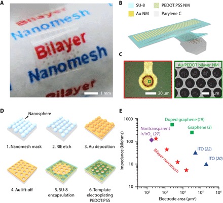
(A) Photograph of a 32-channel Au/PEDOT:PSS nanomesh MEA wrapped on a paper rod. Scale bar, 1 mm. (B) Device schematic of the 32-channel Au/PEDOT:PSS nanomesh MEA in (A). (C) Left: Microscope image of a Au/PEDOT:PSS bilayer-nanomesh microelectrode (20 μm in diameter). Right: SEM image of a zoomed-in region of the microelectrode shown on the left. (D) Fabrication process of the bilayer-nanomesh MEAs. (E) Impedance of different bilayer-nanomesh microelectrodes versus electrode site area. Results from bilayer-nanomesh microelectrodes are benchmarked against the ones from major transparent MEAs from graphene, ITO, and nontransparent Michigan arrays. NM, nanomesh.