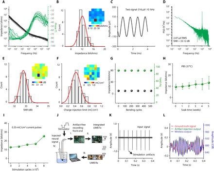
Fig. 2. Bench testing of 32-channel bilayer-nanomesh MEAs.

(A) Impedance magnitude and phase spectra of the 31 working electrodes in a 32-channel Au/PEDOT:PSS bilayer-nanomesh MEA. (B) Electrode impedance histogram of the 32-channel Au/PEDOT:PSS nanomesh MEA in (A). Inset: Impedance colormap with respect to actual channel position. (C) Bench recording output of a 1000-Hz, 316 Vp-p sine wave input using the Au/PEDOT:PSS nanomesh MEA in (A). (D) Power spectra density of recorded sine wave output in (C). (E) SNR histogram from all electrodes with the bench recording in (C). Inset: SNR colormap with respect to actual channel position. (F) Histogram of charge injection limit of all electrodes from the 32-channel Au/PEDOT:PSS nanomesh MEA in (A). Inset: Charge injection limit color map with respect to actual channel position. (G) Average electrode impedance and array yield as a function of bending cycles with a bending radius of 4 mm. (H) Average electrode impedance as a function of weeks after soaking for devices immersed in PBS (pH 7.4) under 37°C. (I) Electrode impedance as a function of stimulating cycles with current pulses (0.35 mC/cm2). (J) Schematic of the experimental setup of the wireless recording with stimulation artifact rejection with the 32-channel Au/PEDOT:PSS nanomesh MEA. (K) Input neural signal contaminated with large stimulation artifacts. (L) Ground truth neural signal overlapped with artifact rejection output (left y axis) and wireless output (right y axis) for comparison. PSD, power spectra density; Tx, transmitter; Rx, receiver; LSB, least significant bit.
