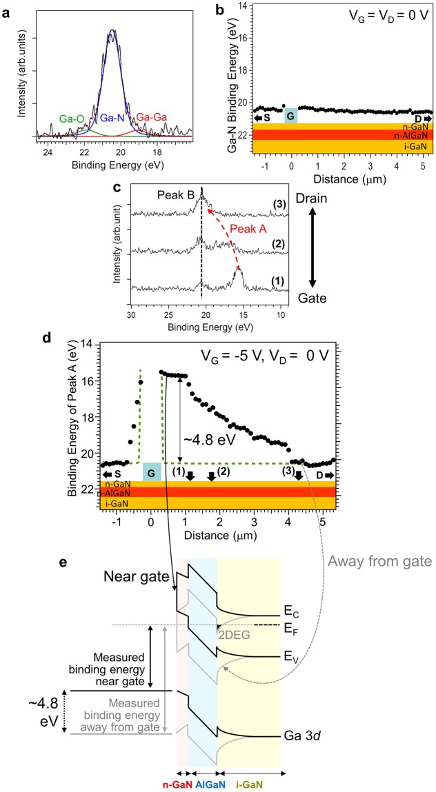
Figure 2.
Operando photoelectron nanospectroscopy measurements of GaN-HEMT surface under gate bias application. (a) Typical Ga 3d spectrum under zero bias application. (b) Line profile of the binding energy of the main Ga–N peak under zero bias application. (c) Spatially resolved Ga 3d spectra under gate bias application. (d) Line profile of the binding energy of the main Ga–N peak under gate bias application. The green dotted line indicates the line profile in the absence of surface electron trapping. (e) Schematic band diagrams near the gate edge (black) and away from the gate edge (gray).

