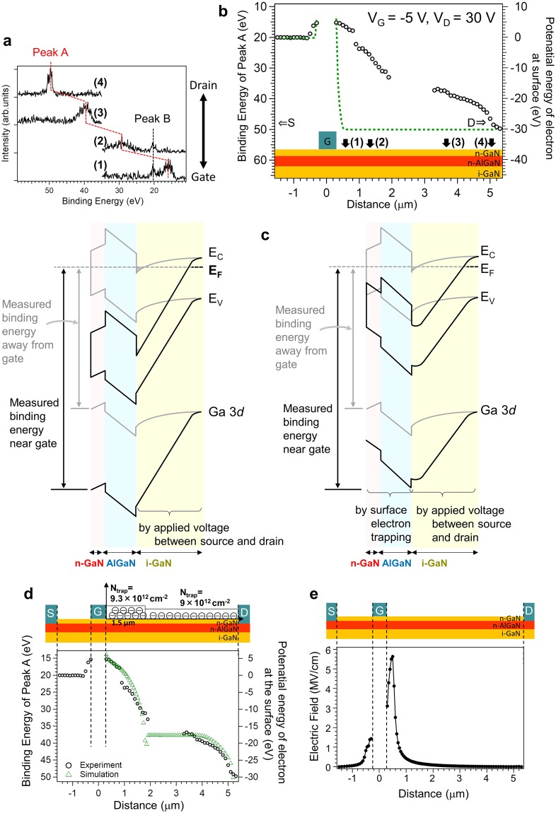
Figure 3.
Operando photoelectron nanospectroscopy results of GaN-HEMT surface under application of both drain and gate biases. (a) Typical Ga 3d spectra under application of drain (30 V) and gate (−5 V) biases. (b) Line profile of the binding energy of the main Ga–N peak under application of drain (30 V) and gate (−5 V) biases. (c) Schematic band diagrams corresponding to (left) absence of surface electron trapping, and (right) occurrence of surface electron trapping. (d) Simulations utilized to reproduce the experimental data by assuming surface electron densities. (e) Estimated local electric field distribution under application of gate (−5 V) and drain (30 V) biases.

