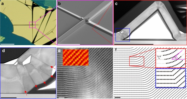
Fig. 1.
Atomic structure of twin boundaries in layered vdW crystals, a Optical plan view image of a 200 nm thick graphite flake on silicon wafer. Stress induced kink bands can be seen intersecting one another at angular multiples of 30° (corresponding to zig-zag, zz, or armchair, ac, crystal directions). Scale bar 100 μm. b Scanning electron microscopy (SEM) oblique view of zz kink band meeting an ac kink band at 90°. The site of the FIB cross-section is annotated red. Scale bar 10 μm. c, d Bright field STEM cross-sectional imaging of the ac kink band. The kink is composed of flat areas of Bernal stacking bordered by many discrete boundaries of almost exactly the same angle, (boundaries annotated with red arrows) which are identified as incommensurate twin boundaries (see SI). Scale bars 1 μm and 100 nm, respectively. e Filtered atomic resolution image of a twin boundary in hBN. The inset shows perfect atomic AA’ stacking is maintained either side (parent and twin lattices) of the twin boundary. The core of the boundary is composed of a volume of crystal, which bends like a nanotube and is incommensurately stacked. Scale bar 1 nm. f Atomic model schematic comparing the delocalised incommensurate twin boundary structure (main figure and upper panel inset) with the conventional abrupt twin boundary (lower panel inset). The parameters that govern twin geometry, slip length L and the ideal twin angle θt are annotated (Table 1). Scale bar 1 nm

