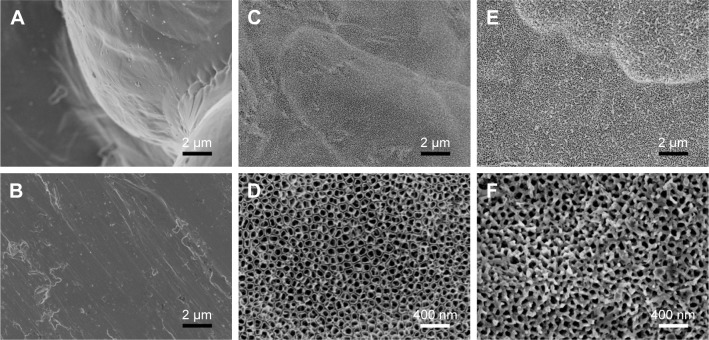
Figure 2.
SEM images showing the surface topography of samples (scale bar of A–C, E =2 µm, scale bar of D, F =400 nm).
Notes: (A) SLM sample with unmelted titanium particles and spheres on the rough waving surface; (B) MP sample with flat surface; (C, D) different magnifications of AO sample showing the arranged TiO2 nanotubes; (E, F) different magnifications of AOC sample showing the amorphous nanoparticles embedded in the nanotubes or the interval of nanotubes.
Abbreviations: SEM, scanning electron microscopy; SLM, selective laser melting; MP, mechanically polished; AO, anodic oxidation; AOC, anodic oxidation composited with electrochemical deposition.

