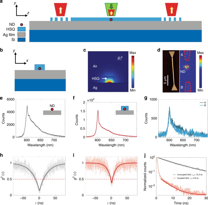
Fig. 3. On-chip direct excitation of a single GeV nanodiamond.
a, b Schematic of a sample layout and the working principle of direct excitation of a GeV nanodiamond embedded in a plasmonic waveguide. c Simulated mode profile for the DLSPP waveguide at λ = 602 nm (GeV ZPL). d AFM image of the fabricated waveguide (left), and CCD camera image of the whole structure where the nanodiamond is excited and a fluorescence image of the focal plane is taken (right). e–g Spectrum taken from uncoupled GeV (e), coupled GeV (f) and outcoupled light through the grating ends A and B (g). The integration time of the spectra is 300 s, and the excitation power is 25 μW. h, i Second order correlation of the GeV centre before (h) and after (i) coupling to the waveguide. j Lifetime of the GeV centre taken before (grey) and after (red) coupling

