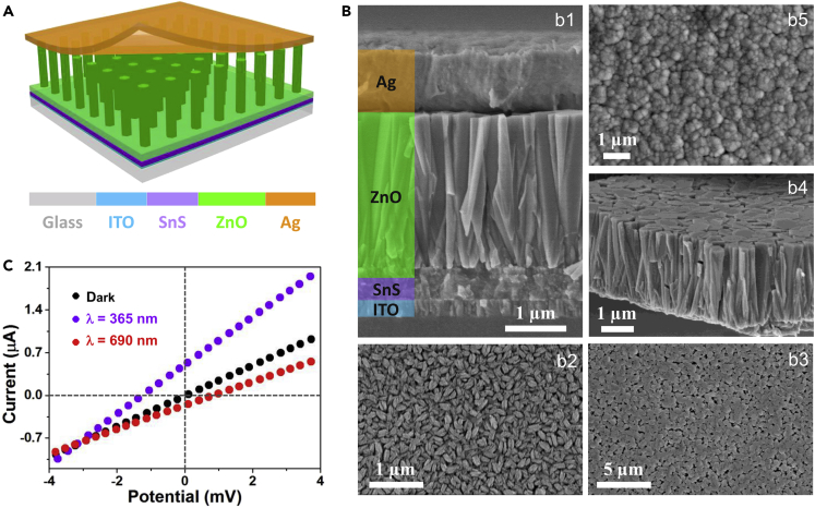
Figure 1.
Structure and Characterization of Self-Powered ZnO NWs/SnS Photodetector
(A) Schematic diagram showing the structure of the photodetector.
(B) SEM image of the ZnO NWs/SnS photodetector: (b1) cross-sectional view of a fabricated device, (b2) top view of the as-deposited shuttle-like SnS nanostructures, (b3) top view of the as-grown ZnO NWs, (b4) tilted cross-sectional view of the ZnO NWs, and (b5) top view of the as-deposited Ag electrode.
(C) I-V characteristics of the device measured under dark, 365 nm light illumination (93.5 mW/cm2), and 690 nm light illumination (23.3 mW/cm2).
See also Figure S1.

