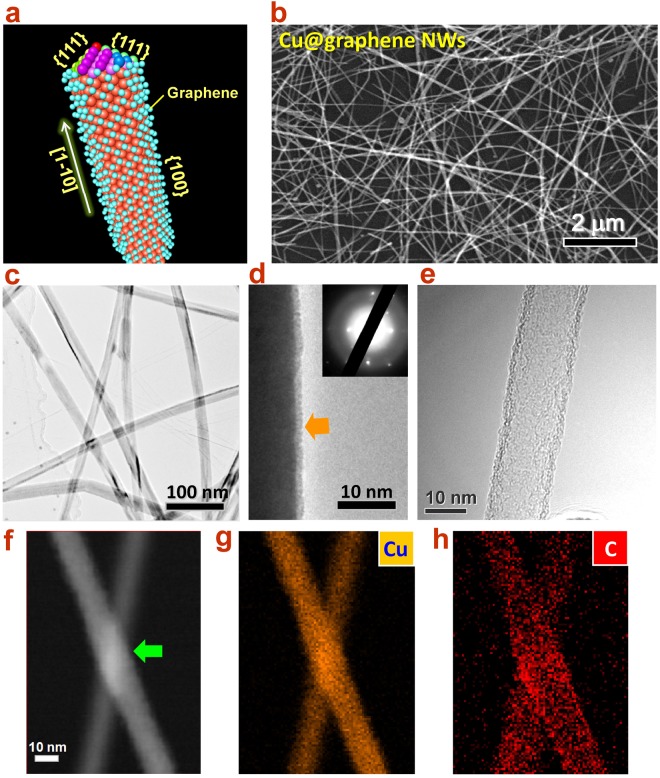
Figure 2.
Graphene encapsulation on Cu NWs. (a) Atomic structure of Cu@graphene NW, where the graphene shell layer is encapsulated on the {100} sidewall of Cu NW. (b) SEM image, (c) TEM image, and (d) high resolution TEM image of Cu@graphene NW. The inset is the SAED image showing the growth direction and structure of Cu@graphene NW. (e) TEM image of free-standing graphene nanotube after the removal of Cu core. (f) Scanning TEM image of interlaced Cu@graphene NWs. The junction is firmly fused after nano-welding treatment. (g) and (h) Elemental mapping images of Cu and C, respectively.

