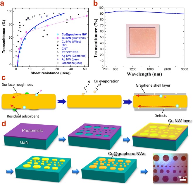
Figure 3.
Optoelectronic performances of Cu@graphene NWs TEs. (a) Transmittance as a function of sheet resistance for various advanced TE materials13,36–41. (b) Optical transmittance spectrum of Cu@graphene NWs film. The inset is the photograph of the Cu@graphene TE film on quartz glass slice. (c) Schematics of electron transport on surface and interface along the Cu@graphene NW. (d) Processing steps of photolithographic patterning of Cu@graphene NW TEs on semiconductor wafer. The last image is the optical micrograph of patterned Cu@graphene NW TE pads in various sizes.

