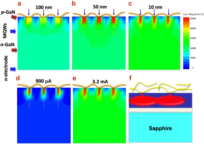
Figure 4.
Current injection and distribution in LED structure with Cu NWs electrodes. Cross-sectional view of color contours of current distribution for Cu NWs in various contact point sizes of (a) 100 nm, (b) 50 nm and (c) 10 nm. Cu NWs are fabricated as the p-GaN electrode with scattered point contacts. Color contours of current distribution for the case of 10-nm contact point size under an injecting current of (d) 900 μA and (e) 3.2 mA. (f) Schematic of current injection and lateral spreading through the nanoscopic contact point at the Cu NW/GaN interface. The high density current injection through the contact point shows a point discharge behavior.

