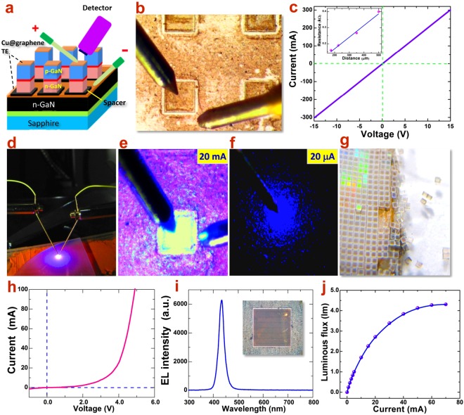
Figure 5.
Transparent LED chips with Cu@graphene NWs electrodes. (a) Structure of GaN-based LEDs on Cu@graphene NW TEs. The placement of probes and detector is setup for electrical and optical measurements. (b) Optical micrograph of patterned LED chips with Cu@graphene NWs. The size of an individual chip is 300 μm by 300 μm. (c) I-V curve of the Cu@graphene NWs electrodes on p-GaN conducting layer. An ohmic contact behavior (linear) could be seen. The inset is the contact resistance as a function of electrode bar distance in the TLM model. (d) Photograph of EL emission of LED chip on Cu@graphene NWs TEs; and (e,f) optical micrographs of the EL emission of the transparent LED chip under working current of 20 mA and 20 μA, respectively. High transparency is achieved without any light blocking. (g) Photograph of laser-cut LED chips array from a 2″ wafer. (h,i) I-V curve and EL spectrum of the transparent LED. A pure and sharp emission at 437 nm is obtained. The inset shows a transparent LED chip in vertical structure by using Cu@graphene NWs TE. (j) Luminous flux as a function of current for the transparent LED.

