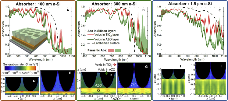
Figure 3.
Optical Response with Optimized Spheroidal Voids Array in TiO2 and AZO
(A–C) Absorption spectra of the LT structures with the design of Figure 1B, corresponding to rows 4 and 5 of Table 1, for the three different absorber layers: (A) 100-nm a-Si, (B) 300-nm a-Si, and (C) 1.5-μm c-Si. The absorption occurring in the Si layer (solid lines) and parasitic losses (colored regions above the lines) are shown for the semi-prolate void arrays incorporated in either a TiO2 (in red) or AZO (in green) front film. The spectra are compared with those (dashed line) calculated in the geometrical optics regime with an ideal Lambertian surface (row 6 of Table 1) instead of the micro-structured film.
(D–I) The bottom profiles show the log-scale generation rate profiles, G, similarly to those of Figure 2. The profiles in (D), (F), and (H) correspond to the void arrays in an AZO film and the profiles in (E), (G), and (I) correspond to those in a TiO2 film, respectively, for the 100-nm a-Si, 300-nm a-Si, and 1.5-μm c-Si absorbers.

