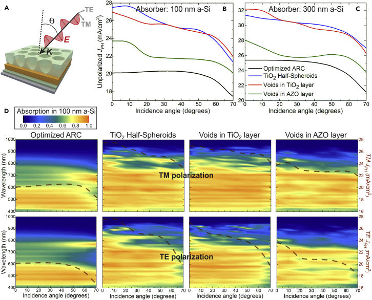
Figure 4.
Angular Study with Optimized Photonic Structures
(A) Sketch of the wave vector (K) and electric field (E) of a TM plane wave incident on the structures at an angle θ with the surface normal (dashed line). The E vector directions in the TM and TE components of unpolarized light are represented by the gray arrows.
(B and C) Angle-resolved unpolarized photocurrent density, JPH, given by the average between the current values attained with the TM and TE polarizations, for the distinct optical structures analyzed in this work on the 100-nm a-Si (B) and 300-nm a-Si (C) absorber layers.
(D) Contour plots of the absorption spectra occurring in the Si material of the 100-nm a-Si cells, as a function of θ, for both TM (top) and TE (bottom) polarization. The dashed brown curve plotted in the contours corresponds to the angle-resolved photocurrent density attained for each case (values in the right axes). See Section S2 in Supplemental Information for further details regarding the angular simulations.

