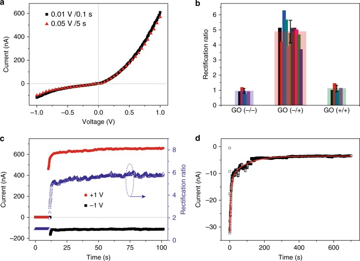
Fig. 2.
Characteization of the graphene pn diode. a The typical current–voltage characteristics of a graphene pn diode with fast (black square, 0.1 V/0.1 s) and slow sweep rate (red triangle, 0.05 V/5 s). b The statistics of rectification ratio of graphene pn diodes (r, approximately 5) and two control experiments composed of either GO(−/−) or GO(+/+) layers, showing no current rectification characteristics (r, approximately 1). The error bar for pn diode is based on 11 devices. The error bars for control experiments are based on five devices. c The current transients were monitored by stepping the potential from 0 to +1 V or −1 V. d The current transients was recorded upon laminating the positively charged and negatively charged GO layers. The current decay was fitted biexponentially

