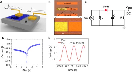
Fig. 5. The device performance of RF rectifiers fabricated using PEDOT-Si Schottky diode.

(A) HF Schottky diode structure composed of high work function metallic oCVD PEDOT thin film and n-type Si. The PEDOT-Si Schottky diode converts the input HF AC signals to DC bias to power a load at its output. (B) Optical image of one representative PEDOT-Si RF diode. The zoom-in figure shows the details. The left terminal is the Schottky junction formed between the PEDOT thin film and Si (Au/Ti/PEDOT/Si); the right terminal is the ohmic electrode on top of Si (Au/Ti/Si). The dashed line indicates the mesa isolation region, where the PEDOT thin film is etched away to isolate each electrode. Scale bar, 10 μm. (C) Equivalent circuit of PEDOT-Si rectifying diode for measurement at 13.56 MHz. The capacitance in the circuit is 0.02 μF. Inductance is 8 mH. The load resistance is adjusted for impedance matching. (D) DC I-V characteristics of the PEDOT-Si diode in the log scale. (E) Rectifying performance of the rectifier. The red line denotes the input AC voltage at the frequency of 13.56 MHz, while the blue line is the output DC voltage rectified by the PEDOT-Si diode. The load resistance used here is 55 kilohms.
