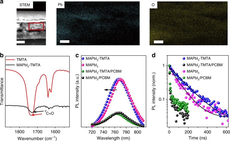
Fig. 3.
TMTA distribution and photoluminescence (PL) characterization. a From left to right, scanning TEM (STEM, scale bar, 200 nm) image and EDS mapping of Pb and O (scale bar, 50 nm). The red line demarcates the EDS mapping area. b Enlarged FTIR spectra of MAPbI3–TMTA and pure TMTA; the arrows indicate the stretching vibration peak of C=O. c Steady-state PL spectra and d time-resolved PL decays of MAPbI3, MAPbI3/PCBM, MAPbI3–TMTA and MAPbI3–TMTA/PCBM. The arrow indicates the blue-shifted PL peak in MAPbI3–TMTA film

