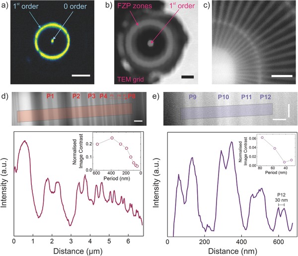
Figure 3.

Synchrotron experiments at BESSY II, UE46‐PGM2. a) Charge coupled device (CCD) image of a scintillator screen showing the 1st order diffraction ring. For this image an order selecting aperture was placed between the FZP and CCD. The scintillator screen was placed further away from the focal point and the image on screen was magnified onto the CCD detector. The ML‐FZP tilt was corrected via a tilt stage until a circular first order focus ring was obtained. The presence of the zero order hints a misalignment of the OSA. The scale bar is 250 nm−1. b) Pinhole scan over the FZP to measure the diffraction efficiency. The transmitted light is collected by an avalanche photo diode (APD). Dwell time 2 ms. Step size 500 nm × 500 nm. Photon energy 1400 eV. Scale bar is 10 µm. c) STXM image of the Siemens Star test pattern. The 30 nm features of the innermost ring are resolved. Dwell time 10 ms. Energy 1198 eV. Step size 10 × 10 nm. Scale bar is 500 nm. d) STXM image of P1 to P8 of the BAM L‐200 test structure (top) and its integrated intensity profile and normalized Michelson image contrast (bottom graph). All features P1 (587 nm)–P8 (48.5 nm) are resolved. Dwell time 10 ms. Step size 10 × 10 nm. Photon energy 1200 eV. Scale bar is 500 nm. e) STXM image of the P9 (76.5 nm) to P12 (30 nm) of the BAM L‐200 test structure (top) and its integrated (15 pixels wide) intensity profile and normalized Michelson image contrast (bottom graph). 30 nm full period structure (P12) is resolved corresponding to 15 nm half‐pitch cut‐off resolution. Dwell time 30 ms. Step size 4 × 5 nm. Photon energy is 1296 eV. Scale bars correspond to horizontal 100 nm and vertical 120 nm.
