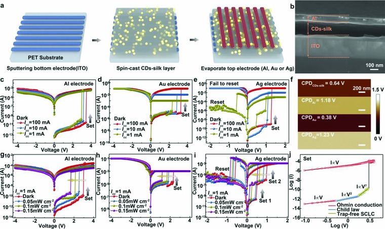
Figure 2.

Device fabrication, structure, and I–V characteristics. a) Schematic illustration depicting the fabrication process of the flexible CDs‐silk memory devices. b) Cross‐sectional SEM image of the device structure. Scale bars: 100 nm. c–e) I–V characteristics of CDs‐silk memories with c) Al, d) Au, and e) Ag top electrode at different positive compliance current (dark, sweeping rate: 50 mV). f) Contact potential difference images from KPFM measurement of CDs‐silk film, Al surface, Au surface, and Ag surface. g–i) I–V characteristics of CDs memories with g) Al, h) Au, and i) Ag top electrode, exposed to UV light (λ = 365 nm) with intensity from 0 to 0.15 mW cm−2 (sweeping rate: 50 mV). j) Experimental data and fitted lines of the I–V characteristics of the Al/CDs‐silk/ITO device at SET process without light irradiation (compliance current: 1 mA).
