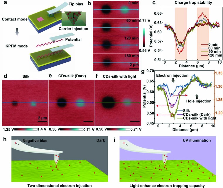
Figure 4.

Charge trapping capability of CDs‐silk film detected by KPFM. a) Schematic representation of experimental setup for 2D injection of electrons or holes into CDs‐silk film in a contact mode, as well as subsequent surface potential measurement in a KPFM mode. A Pt/Ir‐coated conductive tip was used. (Charge injection area: 1 µm; tip bias: ‐6 V or +6 V; charge injections into CDs‐silk film without or with light were conducted by the same method; UV light intensity: 0.15 mW cm−2.) Surface potential images of b) CDs‐silk layer and c) selected cross section as a function of time (0, 60, 120, and 180 min) after charge injection process. Scale bars: 2 µm. Surface potential images of d) silk, e) CDs‐silk without or f) with light irradiation and g) the selected cross sections. Schematic illustration of the process of 2D electron injection to CDs‐silk film h) without and i) with UV illumination using a conductive AFM tip at negative bias.
