Figure 5.

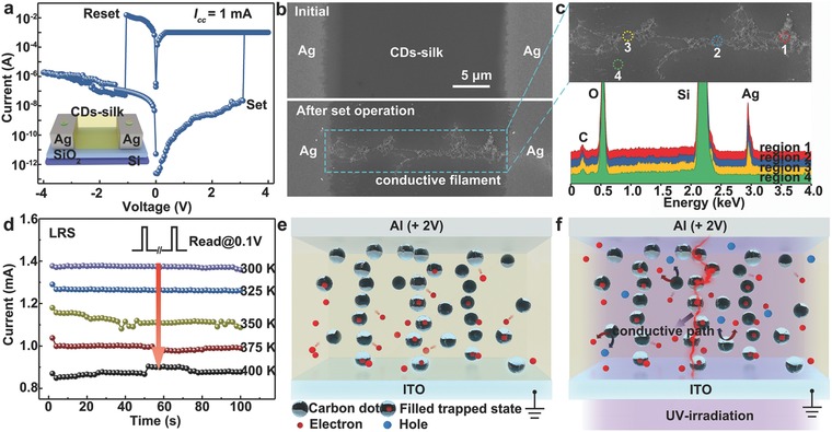
The working principle of CDs‐silk‐based memory device with Ag electrode and the proposed resistive switching mechanism in CDs‐silk‐based memory. a) The SET and RESET operation of a planar Ag/CDs‐silk/Ag device (compliance current: 1 mA, sweeping rate: 50 mV). The inset displays 3D illustration of as‐fabricated planar device. b) SEM images of the planar device before and after SET operation, scale bars: 5 µm. c) An enlarged SEM image of the conductive filament and EDS spectra in different regions. d) The temperature dependence of LRS currents of a vertical Ag/CDs‐silk/ITO device. The devices were measured with constant application of 0.1 V read voltage at 300–400 K. e,f) By application, a positive voltage sweep, the injected charge carrier begin to fill the trapping centers in the CDs‐silk layer. However, the bias (+ 2 V) is not enough to induce a conduction path. In contrast, the charge trapping capacity can be significantly enhanced via photogating effect induced by UV‐irradiation treatment, thus promoting the formation of a conductive path, leading to an abrupt change of device conductivity.
