Figure 2.
Characterization of the MPC
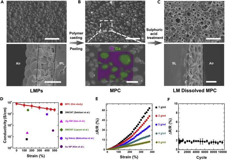
(A) Scanning electron microscopy of LMPs: top, top view; bottom, cross-sectional view. Scale bar, top, 30 μm; bottom, 10 μm. Black dashed line: region of stacked LMPs.
(B) The scanning electron microscopic and elemental analyses of the surface of the MPC. LM islands (green: Ga) in the sea of polymer (purple: Si). Scale bar, top, 30 μm; bottom, 5 μm.
(C) The MPC after dissolving the LM. Top, surface appearance, scale bar, 20 μm; bottom, cross-sectional appearance, scale bar, 10 μm. Dashed line: thickness of the MPC.
(D) Conductivity dependence on tensile strain of printed MPC and comparison with reported printed conductors.
(E) The change of resistance with different strain using MPC patterns printed by inks with different concentrations.
(F) ΔR/R changes with a strain of 50% for 10,000 cycles. Data in (D) and (F) are expressed as mean ± SD.
See also Figures S3 and S4.

