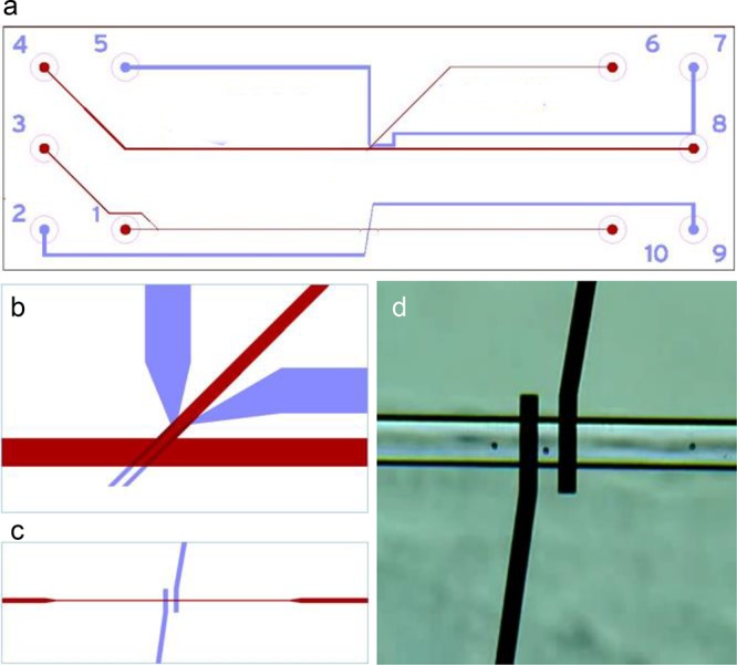
Figure 5.

TCB chip for trapping and counting of beads: (a) Layout of the TCB chip (45 mm long, 15 mm wide). Channels (25 μm deep) are shown in red, with inlets labeled 1 (channel 70 μm wide; near the electrodes 54 μm wide), 3 (channel 70 μm wide), 4 (channel 150 μm wide), outlets labeled 6 (branch 70 μm wide), 8, 10; electrode paths (made of Pt, placed in etched and TiO coated paths) are shown in blue, with connections labeled 2, 5, 7, 9. (b) Layout of the channels and electrodes used for trapping beads or cells (electrode tips 15 μm wide). (c) Tips of the sensing electrodes (tips 25 μm wide) at the bottom of the channel (54 μm wide, as described by Segerink et al.17). (d) Microscopic view of 6 μm beads passing through the channel depicted in part c. The chip is made from borosilicate glass, using positive resist and a wet etching (HF) technique.
