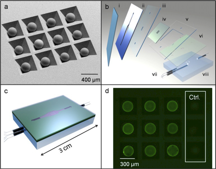
Fig. 8. Schematic diagram of nano-bio chips for cytokines.
(a) SEM photomicrograph of beads in anisotropically etched silicon chip.
(b) Chip (iv) is fitted between double-sided adhesive layer (ii) and cover slip (i) with laminate layers (ii, v, vi) included to direct fluid flow through PMMA base (vii) and inlet and outlet ports (vii).
(c) Sealed LOC assembly.
(d) Fluorescent image of beads after immunoassay including negative controls as imaged with 1 s of CCD camera integration (exposure) time. Adapted from Ref. [91] With permission. (For interpretation of the references to color in this figure legend, the reader is referred to the Web version of this article.)

