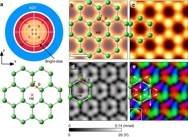
Fig. 1.
Projected atomic electric field maps of monolayer graphene. a Schematic view of the orientation relation between the segmented/ADF detectors and the crystal of monolayer graphene. The yellow disk indicates the bright-field region. b, c Atomic-resolution ADF-STEM image, d projected electric field strength map, and e projected electric field vector map. The contrast range in (d) is 0–20 V or 0–0.14 mrad. The scale bar in (b) is 2 Å

