Figure 7.
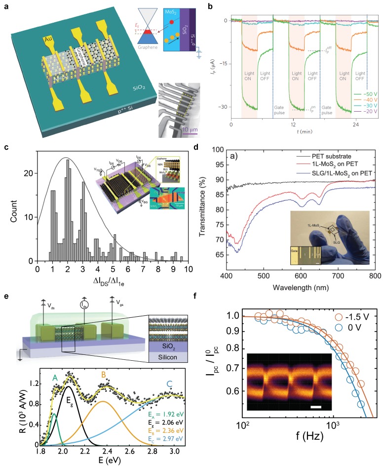
TMD-graphene hybrids. (a) schematic of MoS-graphene photodetector with scanning electron microscope (SEM) image of device (lower inset) and principle of operation (upper inset); (b) temporal response of photocurrent from device in (a) under illumination and gate pulse cycles. Reproduced with permission from Roy et al. [100] Copyright 2013, Nature Publishing Group; (c) histogram of normalized current shift indicating number resolved photon counting. Inset shows schematic and SEM image of device. Reproduced with permission from Roy et al. [101] Copyright 2017, John Wiley & Sons; (d) transmittance of all-chemical vapour deposition (CVD) MoS/graphene photodetector. Optical image highlights transparency (inset). Reproduced with permission under CC-BY 4.0 from De Fazio et al. [103], 2015 ACS Publications (Washington, DC, USA); (e) schematic of ionic polymer gated WS-graphene photodetector (upper) and spectral responsivity (lower); (f) optical bandwidth of device in (e) extends to . Inset shows eye diagram obtained at . Reproduced with permission under CC-BY 4.0 from Mehew et al. [28], 2017 John Wiley & Sons.

