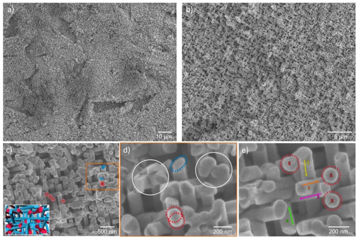
Figure 3.
SEM images of a representative nanowire network with wire diameter ~150 nm and density ~5 × 10⁹ wires/cm2 at (a) low and (b,c) high magnification. The inset in (c) shows a 3D illustration of the top view of the network with wires tilted (blue) and perpendicular (red) with respect to the substrate; (d,e) zoomed-in SEM images of the network showing intersections and wire orientations.

