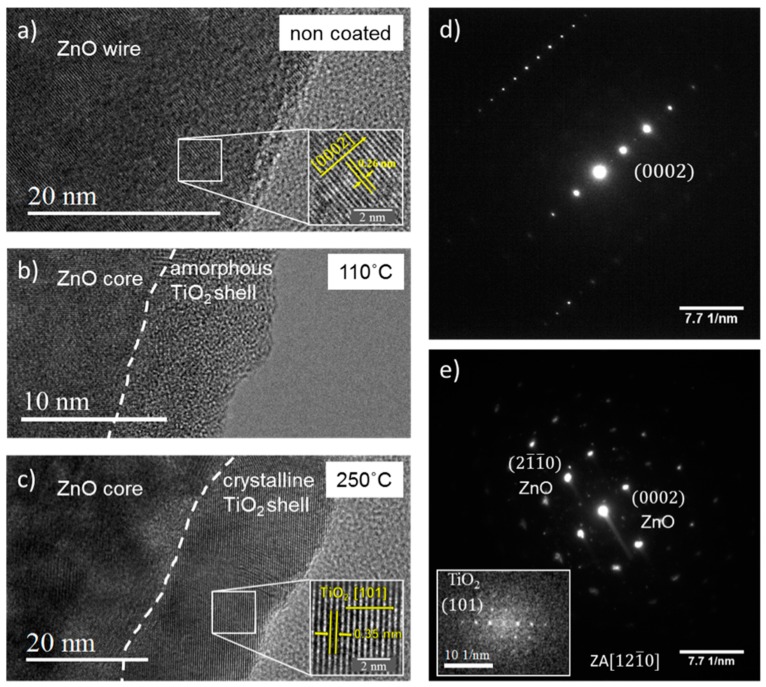
Figure 4.
High resolution transmission electron microscopy (HRTEM) images of (a) ZnO and (b,c) ZnO/TiO2 nanowires. The TiO2 layer was synthesized by ALD at (b) 110°C and (c) 250 °C. The insets show high magnification images with measured d-spacings of 0.26 nm (a) and 0.35 nm (c) corresponding to the crystallographic planes of ZnO (0002) and anatase TiO2 (101), respectively. SAED patterns in (d,e) correspond to the ZnO and ZnO/TiO2 nanowires shown in (a,c), respectively. The inset in (e) shows the Fourier transform image of the crystalline TiO2 shell deposited at 250 °C.

