
Figure 5.
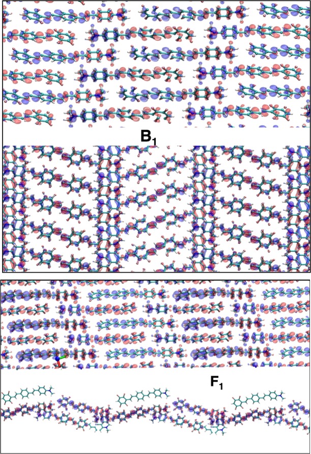
Induced charge densities of the main absorption peaks of Figure 4. (Top panel) Induced charge density of peak B1 of bulk crystal; (bottom panel) induced charge density of peak F1 of monolayer film crystal. For each induced charge density, we have plotted two different side views, one is along the plane where both bulk and film are extended and the other along the plane where the film is confined.