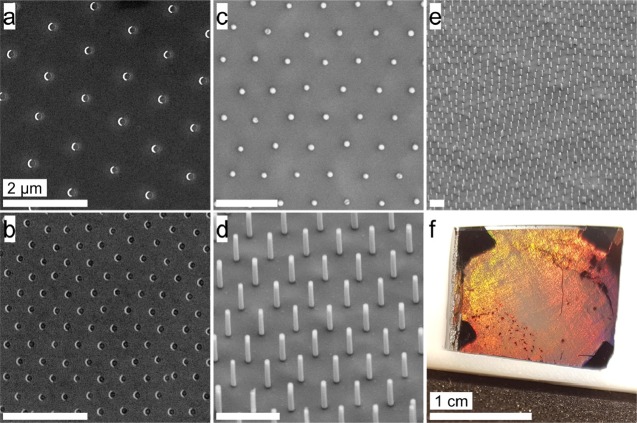
Figure 6.
Applications of non close-packed silica monolayers as templates in colloidal lithography. (a, b) SEM images of Au nanocrescents with different spacings ((a) 1100 nm; (b) 600 nm) but constant dimensions of 160 nm. (c–f) Vertically aligned silicon nanowires etched by metal-assisted chemical etching (MACE). (c) Top view image showing the hexagonal symmetry inherited from the colloidal monolayer template. (d, e) Side-view images tilted by 30°. Scale bars: 2 μm. (f) Macroscopic photograph of the etched silicon wafer. Regions with silicon nanowires show structural coloration. The dark edges correspond to the areas where the substrate was fixed to the stage of the metal evaporator. Scale bar: 1 cm.

