Fig. 1.
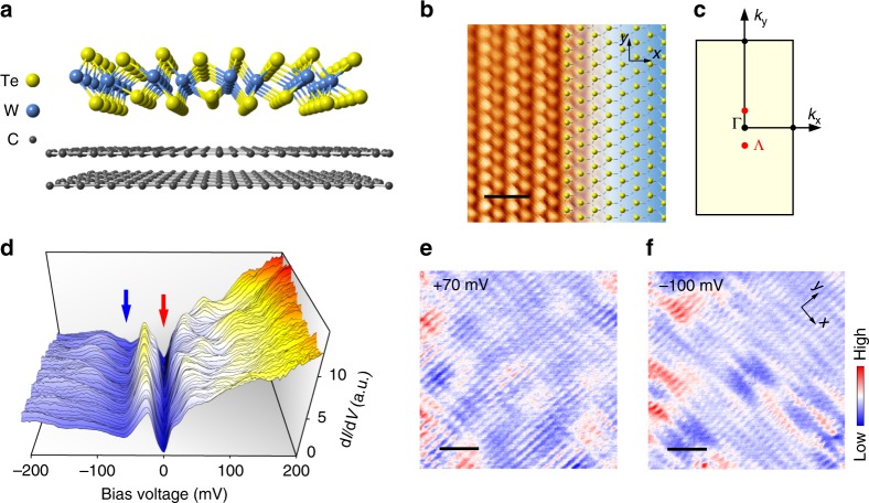
STM topography and dI/dV spectra of single-layer 1T’-WTe2 grown on BLG/SiC(0001). a Atomic model of the single-layer 1T’-WTe2 structure grown on bilayer graphene /SiC substrate. b Atomic resolution STM image of the single-layer 1T’-WTe2 surface (5 × 5 nm2, U = + 15 mV, It = 300 pA). The length of the scale bar is 1.0 nm. The right half of the STM image is overlaid by the lattice of 1T’-WTe2 with the top-layer Te atoms represented by yellow balls. c The corresponding Brillion Zone of single-layer 1T’-WTe2. The locations of the minimum of conduction band are marked by red dots and labeled by Λ. d Spatial variation of dI/dV spectra (U = + 100 mV, It = 200 pA) taken at 128 locations along a line of ~16 nm. The red and blue arrows mark the energy gap at EF, and the intensity minimum. e, f Two typical dI/dV maps (18 × 18 nm2) taken on the single-layer 1T’-WTe2 terrace. U = + 70 mV for e and U = −100 mV for f, It = 100 pA. The length of the scale bar is 3.6 nm. The QPI-induced spatial modulations are clearly identified

